
Media contact: Yvonne Taunton
 Self-assembly techniques using DNA to construct metal nanostructures could allow industrial production of better solar panels and other new technologies, says Krishen Appavoo. "If we can do it with DNA, we can scale it."The metals industry built Birmingham after the Civil War, and biomedical research at UAB helped save the Magic City after the American steel industry collapsed a century later. Now, a UAB physicist is working on a project that ties these two economic pillars together — using DNA.
Everyone benefits when devices get more powerful even as they shrink in size: more efficient solar panels, better pacemakers and cheaper high-definition televisions are just a few examples. Unfortunately, the conventional electronic materials, such as silicon, that have powered the tech revolutions of the past few decades are nearing fundamental performance limits.
Building nanostructures with DNA
That’s where metamaterials — composite materials that don’t occur in nature — come in. They can be designed with all kinds of exotic properties, especially properties that offer new control over light-matter interaction. (Cloaking has attracted plenty of attention, for example.) But creating these intricately layered materials in the lab is expensive and slow, which is a roadblock to commercialization.
With a nearly $250,000 grant from the National Science Foundation, UAB researcher Kannatassen “Krishen” Appavoo, Ph.D., is exploring a new way to accelerate the manufacture of metamaterials: by tapping into the constructive power of DNA. “Our goal is to use DNA strands to create complex assemblies of these nanostructures,” says Appavoo, an assistant professor in the UAB College of Arts and Sciences Department of Physics.
Rerouting light
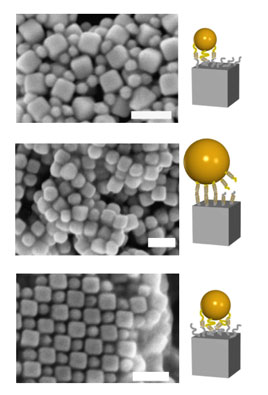 Nano- cubes and spheres are linked by DNA in these scanning electron microscope images from the lab of Oleg Gang, Ph.D., in a Nature Communications paper. The scale bar is 100 nanometers. Images reproduced from Lu, F., Yager, K. G., Zhang, Y., Xin, H. & Gang, O. Superlattices assembled through shape-induced directional binding. Nat Commun 6, (2015).Fabricating nanostructures at extremely high tolerances of shape, size and composition offers control over how a material propagates light, Appavoo explains. A thin film of metamaterials that can harvest or absorb more light than traditional solar panels could be used to increase the efficiency of solar arrays, for instance. Other uses include smaller, lighter satellite antennas and drone-carried sensors.
But widespread commercialization can’t happen if the metamaterials manufacturing process still relies on the very large, expensive pieces of equipment needed for techniques such as electron beam lithography. Oleg Gang, Ph.D., a scientist at Brookhaven National Laboratory on New York’s Long Island, has pioneered a new approach. By binding metal nanostructures to each of the individual bases of DNA, then allowing the bases to form their natural bonds (adenosine with thymine, guanine with cytosine) Gang has been able to create materials that self-assemble into complex structures.
Cutting-edge fields
The NSF funding will allow Appavoo and a graduate student — and potentially undergraduates as well — to travel to Brookhaven to learn the self-assembly technique and apply it to new types of materials. “Right now, there is lots of knowledge about how to bind gold nanoparticles,” Appavoo says. “Our goal is to increase knowledge about how to bind other types of semiconductors in a self-assembled way. If we can do it with DNA, we can scale it.”
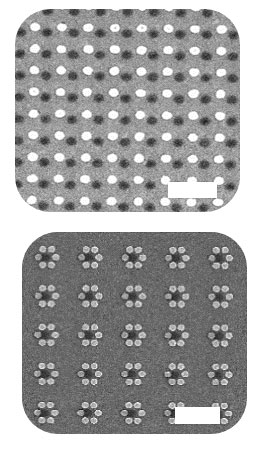 An Appavoo lab image of electron-beam lithography used to make “flat metamaterial.” The scale bar is 1 micrometer.The UAB team will also learn the techniques of electron-beam lithography, and use the lab’s transmission electron microscope to gain more insight on their nanoparticles’ configuration and structure. In addition to the research benefits, this will be invaluable experience for graduates and undergraduates from Alabama in the high-demand fields of photonics, nanofabrication and high-resolution microscopy.
Undergraduates working in Appavoo’s lab already develop expertise in nanofabrication and ultrafast spectroscopy — “essentially time-lapse photography using laser pulses to observe changes in a material in picoseconds, or a millionth of a millionth of a second,” Appavoo says. (Read about undergraduate Appavoo lab member Karly Casey’s summer experience at Brookhaven National Lab on another project.)
Metamaterials on a large scale
The project syncs up with the goals of the Materials Genome Initiative, “a national initiative to increase the pace of advanced-materials discovery, innovation and commercialization,” he adds. Other UAB Physics investigators, including David Hilton, Ph.D., and department chair Ilias Perakis, Ph.D., have contributed research to the Materials Genome Initiative, Appavoo notes. In fact, their work helped attract him to UAB.
If the project is successful, the process could be adapted to high-throughput manufacturing techniques such as slot dye or inkjet printing, says Appavoo. “It will offer a strategy to create metamaterials on a large scale.”